Create
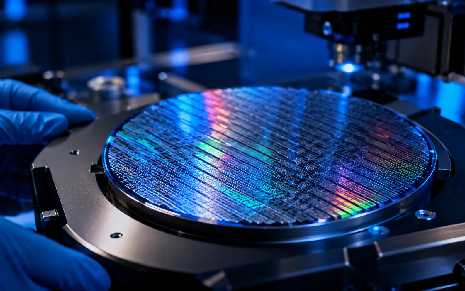
Create the first Prime Wafer: a monolithic, full-spectrum RGB LED semiconductor platform designed for many industries and generations of products.
EXAMPLESDefine The Material StackModel The RGB DeviceDesign The First Test Mask


NASA AWARDED GLOBAL EXCLUSIVITY
The first true MicroLED. NASA awarded Global Photonics Solutions the exclusive global license to the Hybrid Crystal patent portfolio for the development and commercialization of the world’s first monolithic RGB LED semiconductor architecture.
“There are two ways of spreading light: to be the candle or the mirror that reflects it.”
EDITH WHARTON
A RELATIONSHIP BUILT OVER YEARS
NASA’s decision was not the beginning of GPS’s work in light—it was the recognition of a scientific and engineering journey already well underway.
In 2006, Brian G. Evans’s focus turned to photonics and semiconductor technologies, particularly LED packaging and placement. This work led to the creation of Global Photonics Solutions. GPS also began engineering novel custom LED displays—projects that demanded far more than the selection and installation of conventional products.
In 2017, while researching photonics patents, Evans discovered published work originating at NASA’s Langley Research Center. He recognized the extraordinary potential of NASA’s monolithic Hybrid Crystal RGB LED semiconductor architecture and began years of study and sustained engagement with NASA.
In April 2025, Global Photonics Solutions was awarded the exclusive global license to NASA’s monolithic Hybrid Crystal LED semiconductor patent portfolio. This landmark decision marked the first time NASA had granted such exclusivity to a company of GPS’s size. NASA entrusted GPS with assembling the scientific, engineering and manufacturing team required to develop this invention into the world’s first single-embodiment, full-spectrum LED semiconductor—and bring it to commercialization.
THE LICENSED TECHNOLOGY
Today’s RGB MicroLED displays still depend on separately manufactured color devices, mass transfer, color conversion or other forms of assembly. The Hybrid Crystal architecture addresses RGB at the semiconductor level.
NASA’s patented approach brings material systems associated with red, green and blue emission together on a unified, double-sided crystalline platform. GPS holds the exclusive global license to develop, manufacture and commercialize Hybrid Crystal LED semiconductor wafers and devices.
The platform is presently in development. GPS is organizing the technical data, fabrication partners and capital required to produce and validate the first Prime Wafer.
A rhombohedral SiGe (111) integration layer creates a pathway for combining III–V and III–nitride semiconductor families within one monolithic architecture.
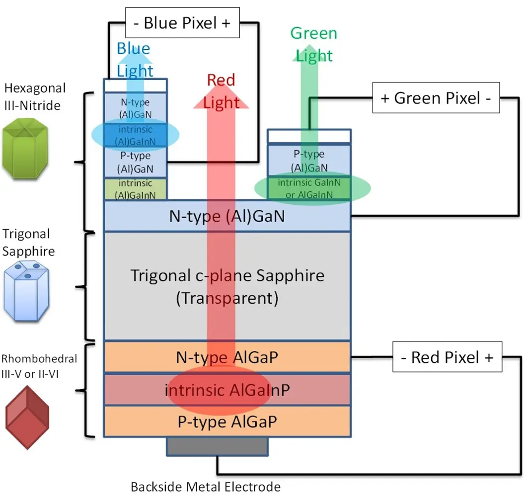 CONCEPTUAL HYBRID CRYSTAL RGB DEVICE STRUCTURE
THE PRIME WAFER PROGRAM
The Prime Wafer will be more than a new semiconductor. It is intended to become the foundation of a new American ecosystem—connecting science, domestic manufacturing, education, investment and products built around a single revolutionary light platform.
Create the first Prime Wafer: a monolithic, full-spectrum RGB LED semiconductor platform designed for many industries and generations of products.
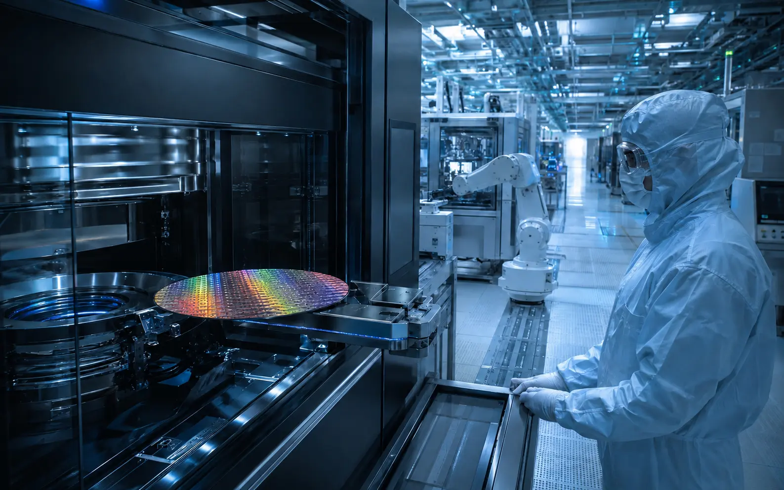
Fabricate, characterize and validate the wafer through American scientific, laboratory, university and semiconductor-foundry partnerships.
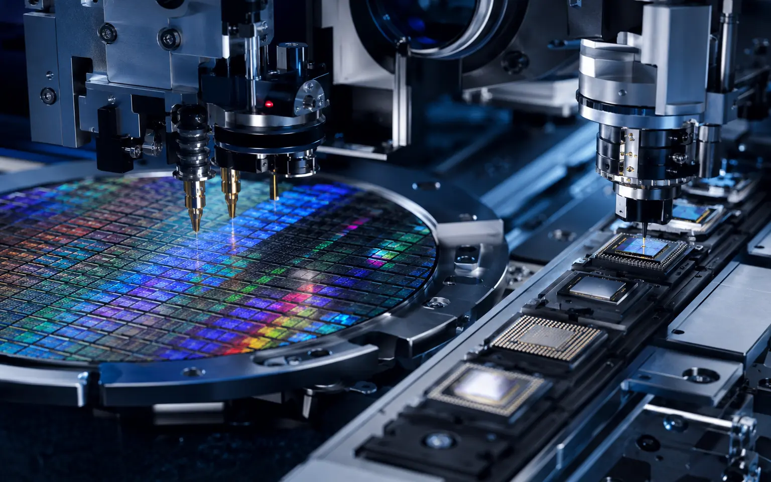
Establish a repeatable U.S. manufacturing pathway spanning epitaxy, devices, packaging, testing and application-specific integration.
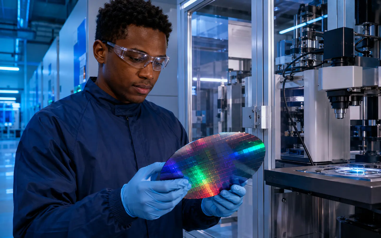
Use the Prime Wafer to fund discovery, develop exceptional semiconductor scientists and seed new companies, products and domestic supply chains.
THE NEW CENTER OF GRAVITY
PLATFORM POTENTIAL
The value of the platform is not limited to a single display. Its material flexibility opens pathways across photonics, communications, sensing and advanced light-based systems.
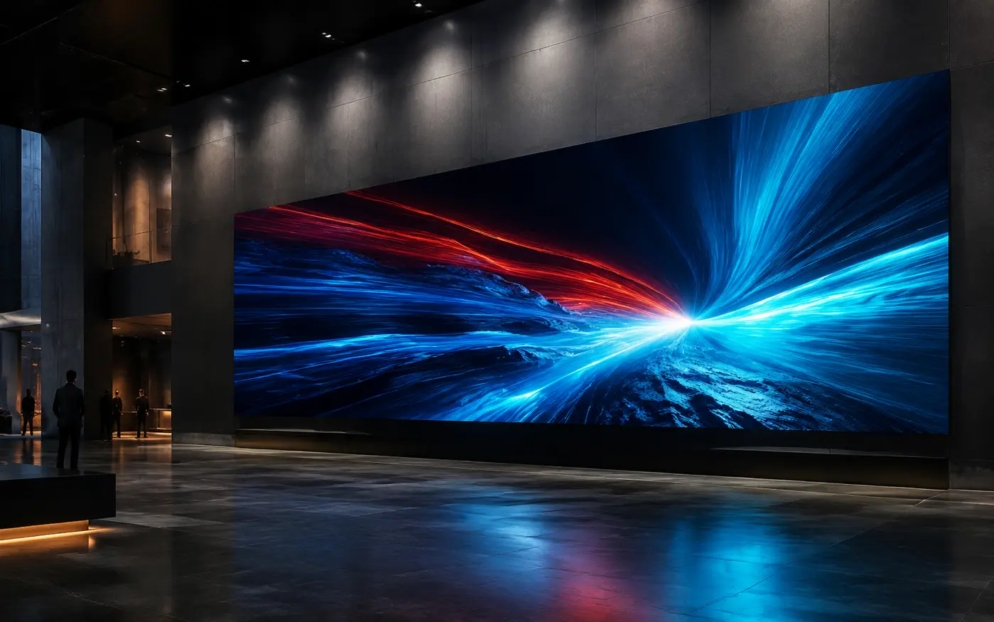
Monolithic RGB architectures for MicroLED, large-format display, AR/VR and next-generation visual systems.

Light-based data pathways for chip-to-chip communication, photonic systems, AI infrastructure and high-performance computing.
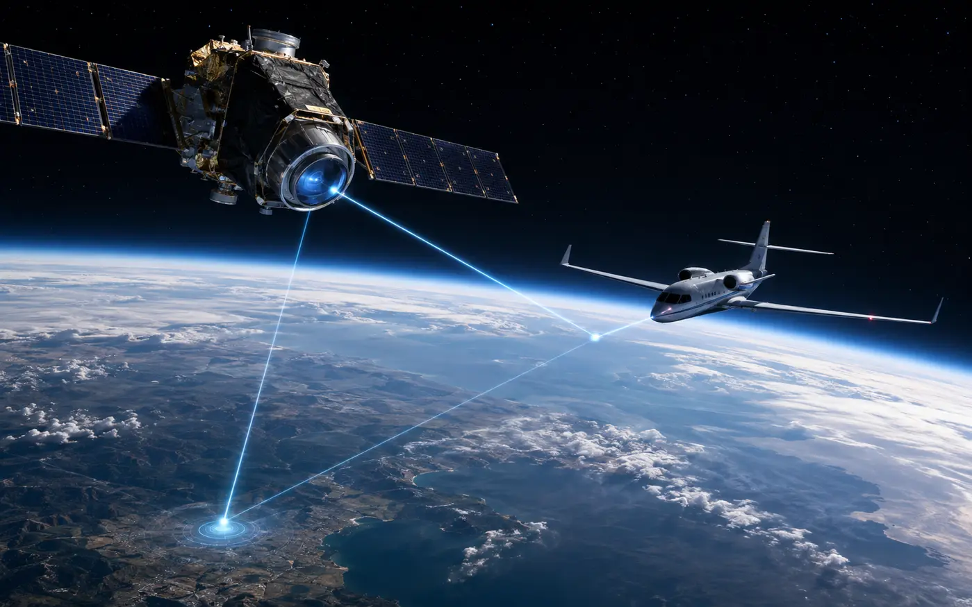
Multi-band emitters for sensing, communications, adaptive systems, situational awareness and mission-specific photonics.

Compact photonic devices for autonomous platforms, Li-Fi, sensing, communications and intelligent transportation.

Potential multi-spectral and miniaturized light sources for imaging, monitoring and analytical instrumentation.

Energy-conscious light engines for smart cities, communication networks and highly integrated electronic systems.
AMERICAN CAPABILITY, BROADLY BUILT
GPS’s vision reaches beyond a single wafer. We intend to help establish a durable American photonics ecosystem—connecting NASA-originated science with national laboratories, domestic foundries, industry and the exceptional talent resident within Historically Black Colleges and Universities.
“We choose to brighten the world,
BRIAN G. EVANS · FOUNDER & CEO
By Nurturing exceptualism to advance in all we do,
We make what happens next!

CUSTOM DISPLAY ENGINEERING
Global Photonics Solutions continues to design and deliver highly customized LED systems for projects that fall outside conventional product catalogs.
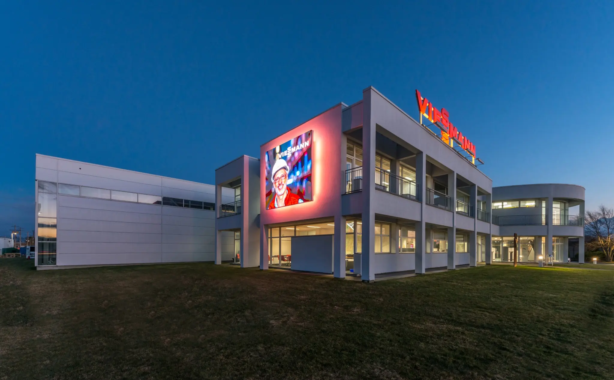
At 8730 Sunset Towers on Sunset Boulevard in West Hollywood, GPS created the custom LED display integrated into the building’s distinctive vertical architectural form. The installation transforms a difficult structure into a commanding digital landmark visible to traffic and pedestrians approaching Sunset Plaza.
Projects like Sunset Worl demonstrate the engineering discipline behind GPS: understanding how light must be packaged, driven, cooled, protected, structurally integrated and delivered as a dependable real-world system.
GPS currently uses Cree LEDs in its custom display systems because their proven durability and longevity support the dependable installations our customers expect.
Once the NASA-GPS LED is fully developed, validated and ready for production, it will become the exclusive LED platform used throughout GPS display systems.
SELECTED GPS WORK
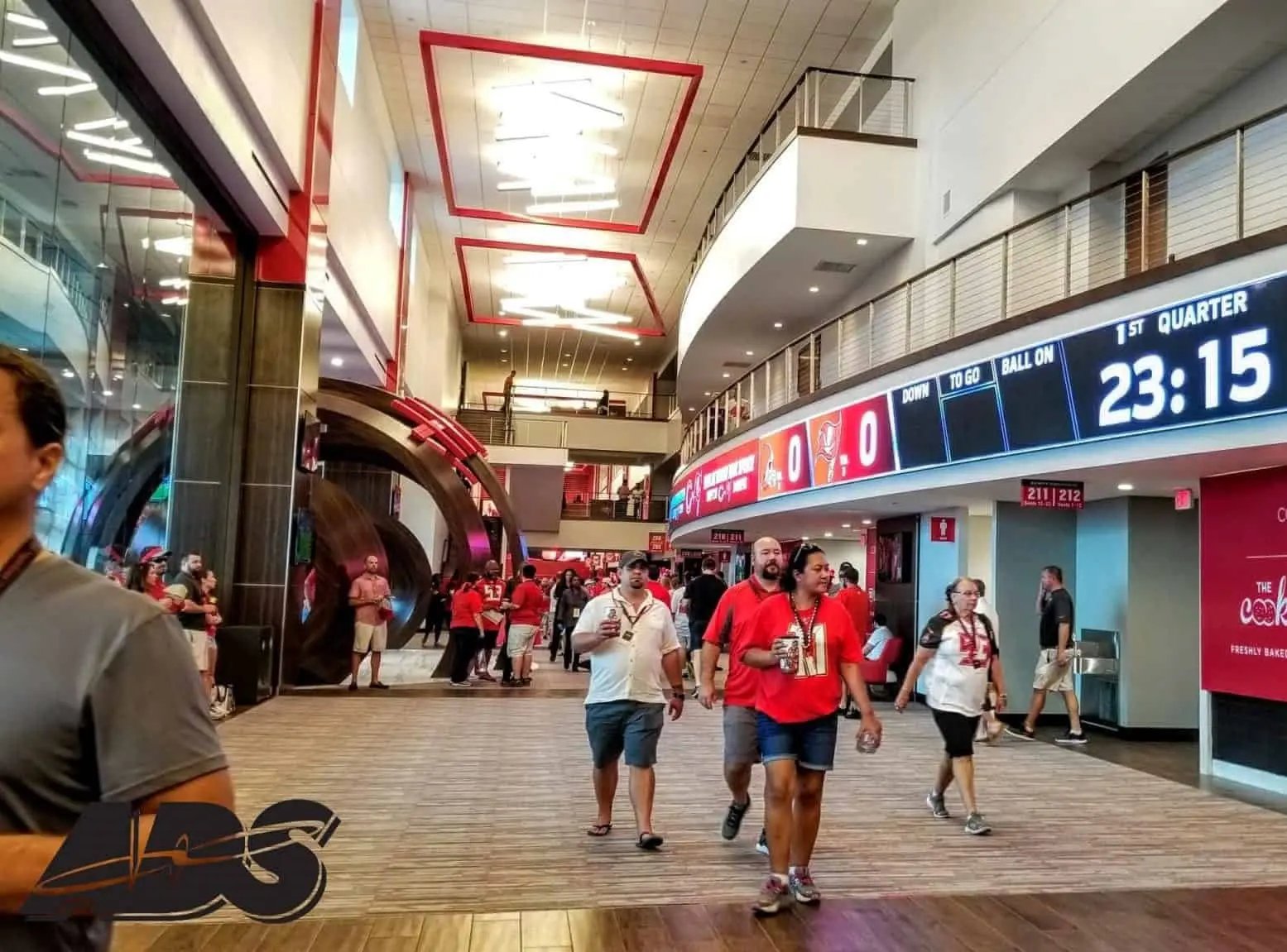
GPS has delivered custom indoor, outdoor, architectural and immersive display systems. Our work extends from corporate environments and galleries to stadiums, entertainment experiences and landmark structures.
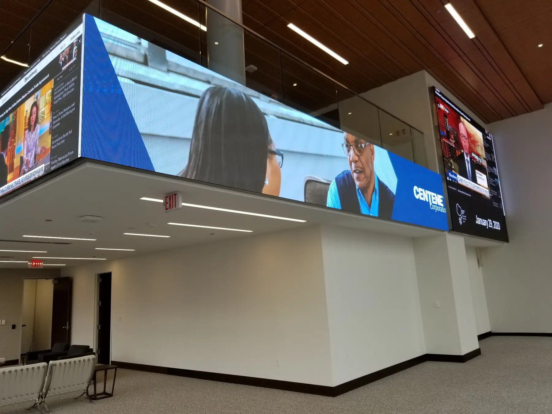
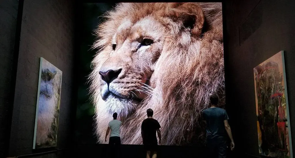

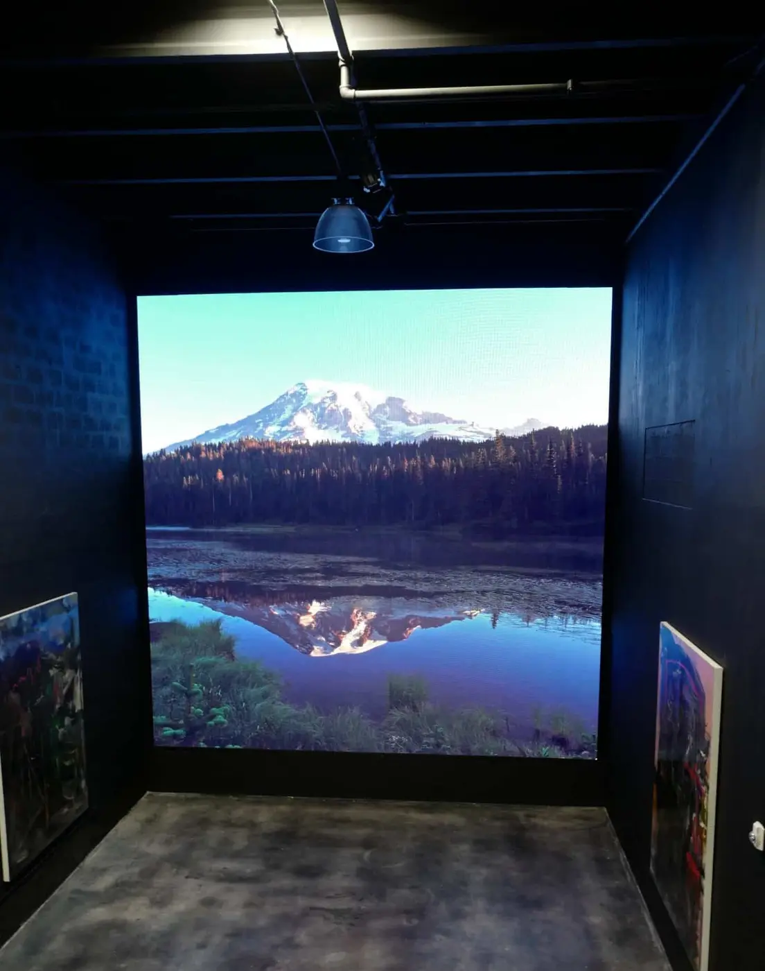
XPERIA combines a walk-through environment with immersive storytelling, interactive moments and CGI animation to bring scientifically inspired ocean encounters to the Smoky Mountains. GPS engineered and supplied the custom display systems that help make the experience feel enveloping and immediate.
SPIE creates, builds and operates large-scale, purpose-built venues with global entertainment and sports franchises. Its work spans concept design, cinematic media, installation and technology integration. GPS supports that ambition with custom display engineering and display systems designed for immersive environments.
WHO WE ARE
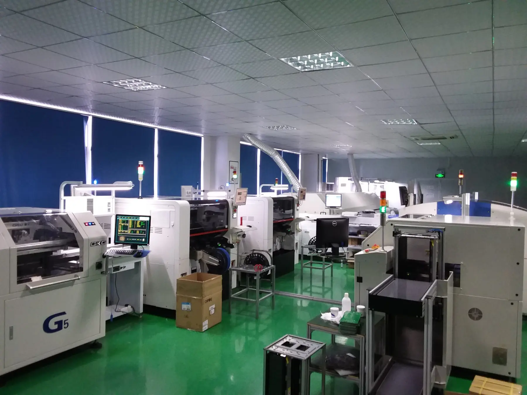
GPS does not approach displays as a commodity. We work from semiconductor, SMT, electronic, mechanical, optical and systems-engineering fundamentals.
Our perspective spans the entire pathway—from LED module manufacturing and detailed cabinet assembly to control, power, thermal management, installation and the semiconductor architecture beneath the light itself.

FOUNDER & CHIEF EXECUTIVE
A scientist, analytical engineer and lifelong maker who has worked across software, electronics, LED manufacturing and advanced semiconductor development.
Evans has spent years inside factories—working beside engineers and technicians, diagnosing problems at their source and turning ambitious concepts into functioning systems. That direct experience now informs GPS’s stewardship of the NASA-GPS Hybrid Crystal technology and the Prime Wafer program.
“We choose to brighten the world,Brian G. Evans, founder and CEO of Global Photonics Solutions.
By Nurturing exceptualism to advance in all we do,
We make what happens next!”

PRESIDENT
Rob brings together a unique combination of financial, sales, and marketing skills to help growth-stage companies build for the long term.
His work spans business strategy, capital formation, and technology licensing, and he uses these skills to help companies raise capital and turn strong ideas into sustainable revenue. While he has worked with businesses at every stage, his primary focus is to help early-stage companies license, commercialize, or scale their technology.
DIRECT CONTACT(602) 295-7377rdspaeth@gpsolutionsled.comSTRATEGIC COLLABORATION
GPS welcomes serious conversations with strategic investors, semiconductor manufacturers, research institutions, government partners and customers pursuing advanced display systems.
DIRECT CONTACTBrian G. EvansBgevans@gpsolutionsled.com(401) 474-8158Begin a conversation ↗Confidential technical information is shared only under appropriate agreements.